Acoustic microscopy
Encyclopedia
Acoustic microscopy is microscopy
that employs very high or ultra high frequency
ultrasound
. Acoustic microscopes operate nondestructively and penetrate most solid materials to make visible image
s of internal features, including defects such as cracks, delaminations and voids.
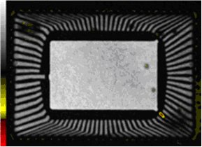
The acoustic image of the plastic-encapsulated IC below was made using a 30 MHz transducer because this frequency provides a good compromise between penetration and image resolution.
In the acoustic image and side-view diagram of the plastic-encapsulated IC to the right, ultrasound was pulsed through the black mold compound (plastic), and reflected from:
The portion of the pulse that is reflected is determined by the “Acoustic Impedance”, Z, of the each material that meets at the interface. The acoustic impedance of a given material is the material’s density multiplied by the speed of ultrasound in that material. When a pulse of ultrasound encounters an interface between two materials, the degree of ultrasonic reflection from that interface is governed by this formula:

where R is the fraction of reflection, and z1 and z2 are the acoustic impedances of the two materials.
If both materials are typical solids, the degree of reflection will be moderate, and a significant portion of the pulse will travel deeper into the sample, where it may be in part reflected by deeper material interfaces. If one of the materials is a gas such as air – as in the case with delaminations, cracks and voids – the degree of reflection at the solid-to-gas interface is near 100%, the amplitude of the reflected pulse is very high, and practically none of the pulse travels deeper into the sample.
In the image of the plastic-encapsulated IC above, gating was on a depth that included the silicon die, the die paddle and the lead frame.

Still scanning the top of the sample, the gating of the return echoes was then changed to include only the plastic encapsulant (mold compound) above the die. The resulting acoustic image is shown above. It shows the structure of the particle-filled plastic mold compound, as well as the circular mold marks at the top surface of the component. The small white features are voids (trapped bubbles) in the mold compound. (These voids are also visible in the previous image as dark acoustic shadows.)

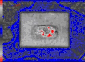
Gating was then changed to include only depth of the die attach material that attaches the silicon die to the die paddle. The die, the die paddle, and other features above and below the die attach depth are ignored. In the resulting acoustic image, shown above slightly magnified, the red areas are voids (defects) in the die attach material.

Finally, the plastic-encapsulated IC was flipped over and imaged from the back side. The return echoes were gated on the depth where the backside mold compound interfaces with the back side of the die paddle. The small black dots in the acoustic image above are small voids (trapped bubbles) in the mold compound.
The scientific literature shows very little progress toward an acoustic microscope following the Dunn and Fry experiments up until about 1970 when two groups of activity emerged, one headed by C.F. Quate (Stanford University) and the other by A. Korpel and L.W. Kessler (Zenith Radio Research Labs). The first efforts to develop an operational acoustic microscope concentrated upon high-frequency adaptations of low-frequency ultrasonic visualization methods. One early system employed Bragg diffraction imaging , which is based upon direct interaction between an acoustic-wave field and a laser light beam. Another example was based on variations of the Pohlman cell . The original device is based upon a suspension of asymmetric particles in a thin fluid layer which, when acted upon by acoustic energy, produce visual reflectivity changes. Cunningham and Quate modified this by suspending tiny latex spheres in a fluid. Acoustic pressure caused population shifts which were visually detectable. Kessler and Sawyer developed a liquid crystal cell that enabled sound to be detected by hydrodynamic orientation of the fluid. In 1973, the Quate group began the development of a concept, which utilized a confocal pair of acoustic lenses for focusing and detecting the ultrasonic energy. Advancements of this instrument, a scanning acoustic microscope, have to do with achieving very high resolution, novel modes of imaging, and applications. The SAM was commercially introduced by Leitz Corp and by Olympus Corp. In 1970, the Korpel and Kessler group began to pursue a scanning laser detection system for acoustic microscopy. In 1974, the activity was shifted to another organization under Kessler (Sonoscan Inc), where practical aspects of the instrument were developed. This instrument, the scanning laser acoustic microscope (SLAM), was made commercial available in 1975.
In 1984, Kessler’s group completed development of the C-SAM concept instrument which operated in the reflection mode, as well as the through-transmission (only) mode of the SLAM. Using the same transducer to pulse ultrasound and receive the return echoes meant that the acoustic image could easily be constrained to a depth of interest. This design was the precursor of essentially all of the acoustic microscopes in use today, and was the development that made possible numerous later advances such as cross-sectional acoustic imaging, three-dimensional acoustic imaging, and others.
Because of their ability to find visualize features nondestructively, acoustic microscopes are widely used in the production of electronic components and assemblies for quality control, reliability and failure analysis. Usually the interest is in finding and analyzing internal defects such as delaminations, cracks and voids, although an acoustic microscope may also be used simply to verify (by material characterization or imaging, or both) that a given part or a given material meets specifications or, in some instances, is not counterfeit. Acoustic microscopes are also used to image printed circuit boards and other assemblies.
There are in addition numerous applications outside of electronics. The assembly of numerous medical products uses acoustic microscopes to investigate internal bonds and features. For example, a polymer film may be imaged to examine its bond to a multi-channel plastic plate used in blood analysis. In many industries, products that involve tubing, ceramic materials, composite materials or some types of welds may be imaged acoustically.
Microscopy
Microscopy is the technical field of using microscopes to view samples and objects that cannot be seen with the unaided eye...
that employs very high or ultra high frequency
Ultra high frequency
Ultra-High Frequency designates the ITU Radio frequency range of electromagnetic waves between 300 MHz and 3 GHz , also known as the decimetre band or decimetre wave as the wavelengths range from one to ten decimetres...
ultrasound
Ultrasound
Ultrasound is cyclic sound pressure with a frequency greater than the upper limit of human hearing. Ultrasound is thus not separated from "normal" sound based on differences in physical properties, only the fact that humans cannot hear it. Although this limit varies from person to person, it is...
. Acoustic microscopes operate nondestructively and penetrate most solid materials to make visible image
Image
An image is an artifact, for example a two-dimensional picture, that has a similar appearance to some subject—usually a physical object or a person.-Characteristics:...
s of internal features, including defects such as cracks, delaminations and voids.
Types of acoustic microscopes
In the half-century since the first experiments directly leading to the development of acoustic microscopes, at least three basic types of acoustic microscope have been developed. These are the scanning acoustic microscope (SAM), scanning laser acoustic microscope (SLAM), and C-mode scanning acoustic microscope (C-SAM). For details of development see the History section below. Since the vast majority of acoustic microscopes in use today are C-SAM type instruments, this discussion will be limited to these instruments.Behavior of ultrasound in materials
Ultrasound is broadly defined as any sound having a frequency above 20 kHz, which is approximately the highest frequency that can be detected by the human ear. However, the acoustic microscopes emit ultrasound ranging from 5 MHz to beyond 400 MHz so that micrometre size resolution can be achieved. The ultrasound that penetrates a sample may be scattered, absorbed or reflected by the internal features or the material itself. These actions are analogous to the behavior of light. Ultrasound that is reflected from an internal feature, or (in some applications) that has traveled through the entire thickness of the sample, is used to make acoustic images.Sample types and preparation
Samples need no special treatment before acoustic imaging, but they should be able to withstand at least brief exposure to water or to another fluid, since air is a very poor transmitter of high frequency acoustic energy from the transducer. The sample may be completely immersed in the water, or scanned with a narrow stream of water. Alternately, alcohols and other fluids can be used so as to not contaminate the sample. Samples typically have at least one flat surface that can be scanned, although cylindrical and spherical samples can also be scanned with the proper fixtures. In the following paragraphs, the sample being described is a plastic-encapsulated integrated circuit.Ultrasonic frequencies
The ultrasonic frequencies pulsed into samples by the transducers of acoustic microscopes range from a low of 10 MHz (rarely, 5 MHz) to a high of 400 MHz or more. Across this spectrum of frequencies there is a trade-off of penetration and resolution. Ultrasound at low frequencies such as 10 MHz penetrates deeper into materials than ultrasound at higher frequencies, but the spatial resolution of the acoustic image is less. On the other hand, ultrasound at very high frequencies do not penetrate deeply, but provide acoustic images having very high resolution. The frequency chosen to image a particular sample will depend on the geometry of the part and on the materials involved.The acoustic image of the plastic-encapsulated IC below was made using a 30 MHz transducer because this frequency provides a good compromise between penetration and image resolution.
Scanning process
The ultrasonic transducer raster-scans the top surface of the sample. Several thousand pulses enter the sample each second. Each pulse may be scattered or absorbed in passing through homogeneous parts of the sample. At material interfaces, a portion of the pulse is reflected back to the transducer, where it is received and its amplitude recorded.In the acoustic image and side-view diagram of the plastic-encapsulated IC to the right, ultrasound was pulsed through the black mold compound (plastic), and reflected from:
- the interface between the overlying mold compound and the top surface of the silicon die.
- the interface between the overlying mold compound and the top surface of the die paddle.
- the interface between the overlying mold compound and delaminations (red) on top of the die paddle.
- the interface between the overlying mold compound and the outer portion (lead fingers) of the lead frame.
The portion of the pulse that is reflected is determined by the “Acoustic Impedance”, Z, of the each material that meets at the interface. The acoustic impedance of a given material is the material’s density multiplied by the speed of ultrasound in that material. When a pulse of ultrasound encounters an interface between two materials, the degree of ultrasonic reflection from that interface is governed by this formula:

where R is the fraction of reflection, and z1 and z2 are the acoustic impedances of the two materials.
If both materials are typical solids, the degree of reflection will be moderate, and a significant portion of the pulse will travel deeper into the sample, where it may be in part reflected by deeper material interfaces. If one of the materials is a gas such as air – as in the case with delaminations, cracks and voids – the degree of reflection at the solid-to-gas interface is near 100%, the amplitude of the reflected pulse is very high, and practically none of the pulse travels deeper into the sample.
Gating of the return echoes
A pulse of ultrasound from the transducer might travel nanoseconds or microseconds to reach an internal interface and be reflected back to the transducer. If there are several internal interfaces at different depths, the echoes will arrive at the transducer at different times. Planar acoustic images do not often use all return echoes from all depths to make the visible acoustic image. Instead, a time window is created that accepts only those return echoes from the depth of interest. This process is known as “gating” the return echoes.In the image of the plastic-encapsulated IC above, gating was on a depth that included the silicon die, the die paddle and the lead frame.

Still scanning the top of the sample, the gating of the return echoes was then changed to include only the plastic encapsulant (mold compound) above the die. The resulting acoustic image is shown above. It shows the structure of the particle-filled plastic mold compound, as well as the circular mold marks at the top surface of the component. The small white features are voids (trapped bubbles) in the mold compound. (These voids are also visible in the previous image as dark acoustic shadows.)

Gating was then changed to include only depth of the die attach material that attaches the silicon die to the die paddle. The die, the die paddle, and other features above and below the die attach depth are ignored. In the resulting acoustic image, shown above slightly magnified, the red areas are voids (defects) in the die attach material.

Finally, the plastic-encapsulated IC was flipped over and imaged from the back side. The return echoes were gated on the depth where the backside mold compound interfaces with the back side of the die paddle. The small black dots in the acoustic image above are small voids (trapped bubbles) in the mold compound.
Other image types
The acoustic images shown above are all planar images, so named because they make visible a horizontal plane within the sample. The acoustic data received in the return echo signals can also be used to make other types of images, including three-dimensional images, cross-sectional images, and thru-scan images. Some of these types are illustrated in the Photo Gallery.History
The notion of acoustic microscopy dates back to 1936 when S. Ya. Sokolov proposed a device for producing magnified views of structure with 3-GHz sound waves. However, due to technological limitations at the time, no such instrument could be constructed, and it was not until 1959 that Dunn and Fry performed the first acoustic microscopy experiments, though not at very high frequencies.The scientific literature shows very little progress toward an acoustic microscope following the Dunn and Fry experiments up until about 1970 when two groups of activity emerged, one headed by C.F. Quate (Stanford University) and the other by A. Korpel and L.W. Kessler (Zenith Radio Research Labs). The first efforts to develop an operational acoustic microscope concentrated upon high-frequency adaptations of low-frequency ultrasonic visualization methods. One early system employed Bragg diffraction imaging , which is based upon direct interaction between an acoustic-wave field and a laser light beam. Another example was based on variations of the Pohlman cell . The original device is based upon a suspension of asymmetric particles in a thin fluid layer which, when acted upon by acoustic energy, produce visual reflectivity changes. Cunningham and Quate modified this by suspending tiny latex spheres in a fluid. Acoustic pressure caused population shifts which were visually detectable. Kessler and Sawyer developed a liquid crystal cell that enabled sound to be detected by hydrodynamic orientation of the fluid. In 1973, the Quate group began the development of a concept, which utilized a confocal pair of acoustic lenses for focusing and detecting the ultrasonic energy. Advancements of this instrument, a scanning acoustic microscope, have to do with achieving very high resolution, novel modes of imaging, and applications. The SAM was commercially introduced by Leitz Corp and by Olympus Corp. In 1970, the Korpel and Kessler group began to pursue a scanning laser detection system for acoustic microscopy. In 1974, the activity was shifted to another organization under Kessler (Sonoscan Inc), where practical aspects of the instrument were developed. This instrument, the scanning laser acoustic microscope (SLAM), was made commercial available in 1975.
In 1984, Kessler’s group completed development of the C-SAM concept instrument which operated in the reflection mode, as well as the through-transmission (only) mode of the SLAM. Using the same transducer to pulse ultrasound and receive the return echoes meant that the acoustic image could easily be constrained to a depth of interest. This design was the precursor of essentially all of the acoustic microscopes in use today, and was the development that made possible numerous later advances such as cross-sectional acoustic imaging, three-dimensional acoustic imaging, and others.
Range of applications
The samples imaged by acoustic microscopes are typically assemblies of one or more solid materials that have at least one surface that is either flat or regularly curved. The depth of interest may involve an internal bond between materials, or a depth at which a defect may occur in a homogeneous material. In addition, samples may be characterized without imaging to determine, e.g., their acoustic impedance.Because of their ability to find visualize features nondestructively, acoustic microscopes are widely used in the production of electronic components and assemblies for quality control, reliability and failure analysis. Usually the interest is in finding and analyzing internal defects such as delaminations, cracks and voids, although an acoustic microscope may also be used simply to verify (by material characterization or imaging, or both) that a given part or a given material meets specifications or, in some instances, is not counterfeit. Acoustic microscopes are also used to image printed circuit boards and other assemblies.
There are in addition numerous applications outside of electronics. The assembly of numerous medical products uses acoustic microscopes to investigate internal bonds and features. For example, a polymer film may be imaged to examine its bond to a multi-channel plastic plate used in blood analysis. In many industries, products that involve tubing, ceramic materials, composite materials or some types of welds may be imaged acoustically.

