Die preparation
Encyclopedia

Wafer (electronics)
A wafer is a thin slice of semiconductor material, such as a silicon crystal, used in the fabrication of integrated circuits and other microdevices...
is prepared for IC packaging and IC testing. The process of die preparation typically consists of 2 steps: wafer mounting and wafer dicing
Wafer dicing
Wafer dicing is the process by which die are separated from a wafer of semiconductor following the processing of the wafer. The dicing process can be accomplished by scribing and breaking, by mechanical sawing or by laser cutting...
.
Wafer mounting
Wafer mounting is a step that is performed during the dieDie (integrated circuit)
A die in the context of integrated circuits is a small block of semiconducting material, on which a given functional circuit is fabricated.Typically, integrated circuits are produced in large batches on a single wafer of electronic-grade silicon or other semiconductor through processes such as...
preparation of a wafer
Wafer (electronics)
A wafer is a thin slice of semiconductor material, such as a silicon crystal, used in the fabrication of integrated circuits and other microdevices...
as part of the process of semiconductor fabrication
Semiconductor fabrication
Semiconductor device fabrication is the process used to create the integrated circuits that are present in everyday electrical and electronic devices. It is a multiple-step sequence of photolithographic and chemical processing steps during which electronic circuits are gradually created on a wafer...
. During this step, the wafer is mounted on a plastic tape that is attached to a ring. Wafer mounting is performed right before the wafer is cut into separate dies
Die (integrated circuit)
A die in the context of integrated circuits is a small block of semiconducting material, on which a given functional circuit is fabricated.Typically, integrated circuits are produced in large batches on a single wafer of electronic-grade silicon or other semiconductor through processes such as...
. The adhesive film on which the wafer is mounted ensures that the individual dies remain firmly in place during 'dicing', as the process of cutting the wafer is called.
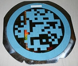
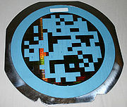
The picture on the right shows a 300 mm wafer after it was mounted and diced. The blue plastic is the adhesive tape. The wafer is the round disc in the middle. In this case, a large number of dies were already removed.
Semiconductor-die cutting
In the manufacturing of micro-electronic devices, die cutting, dicing or singulation is a process of reducing a waferWafer (electronics)
A wafer is a thin slice of semiconductor material, such as a silicon crystal, used in the fabrication of integrated circuits and other microdevices...
containing multiple identical integrated circuits to individual dies each containing one of those circuits.
During this process, a wafer with up to thousands of circuits is cut into rectangular pieces, each called a die. In between those functional parts of the circuits, a thin non-functional spacing is foreseen where a saw can safely cut the wafer without damaging the circuits. This spacing is called scribe line or saw street. The width of the scribe is very small, typically around 100 μm
Micrometre
A micrometer , is by definition 1×10⁻⁶ of a meter .In plain English, it means one-millionth of a meter . Its unit symbol in the International System of Units is μm...
. A very thin and accurate saw is therefore needed to cut the wafer into pieces. Usually the dicing is performed with a water-cooled circular saw with diamond-tipped teeth.
Types of blades
The most common make up of blade used is either a metal or resin bond containing abrasive grit of natural or more commonly synthetic diamond, or borazon in various forms. Alternatively, the bond and grit may be applied as a coating to a metal former. See diamond toolsDiamond tools
A diamond tool is a cutting tool with diamond grains fixed on the functional parts of the tool via a bonding material or another method. As diamond is a superhard material, diamond tools have many advantages as compared with tools made with common abrasives such as corundum and silicon...
.

