Heterojunction bipolar transistor
Encyclopedia
The heterojunction
bipolar transistor (HBT) is a type of bipolar junction transistor
(BJT) which uses differing semiconductor materials for the emitter and base regions, creating a heterojunction. The HBT improves on the BJT in that it that can handle signals of very high frequencies, up to several hundred GHz. It is commonly used in modern ultrafast circuits, mostly radio-frequency (RF) systems, and in applications requiring a high power efficiency, such as RF power amplifiers in cellular phones. The idea of employing a heterojunction is as old as the conventional BJT, dating back to a patent from 1951.
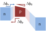
 The principal difference between the BJT and HBT is in the use of differing semiconductor materials for the emitter and base regions, creating a heterojunction. The effect is to limit the injection of holes from the base into the emitter region, since the potential barrier in the valence band is higher than in the conduction band. Unlike BJT technology, this allows a high doping density to be used in the base, reducing the base resistance while maintaining gain. The efficiency of the heterojunction is measured by the Kroemer factor, named after Herbert Kroemer
who was awarded a Nobel Prize
for his work in this field in 2000 at the University of California, Santa Barbara.
Materials used for the substrate include silicon, gallium arsenide, and indium phosphide, while silicon / silicon-germanium alloys
, aluminium gallium arsenide
/ gallium arsenide, and indium phosphide / indium gallium arsenide
are used for the epitaxial layers. Wide-bandgap semiconductors are especially promising, e.g. gallium nitride and indium gallium nitride
.
In SiGe
graded heterostructure transistors, the amount of germanium in the base is graded, making the bandgap narrower at the collector than at the emitter. That tapering of the bandgap leads to a field-assisted transport in the base, which speeds transport through the base and increases frequency response.
is principally employed. In addition to base, emitter and collector layers, highly doped layers are deposited on either side of collector and emitter to facilitate an ohmic contact
, which are placed on the contact layers after exposure by photolithography
and etching. The contact layer underneath the collector, named subcollector, is an active part of the transistor.
Other techniques are used depending on the material system. IBM and others use UHV CVD for SiGe; other techniques used include MOVPE for III-V systems.
, built from indium phosphide and indium gallium arsenide
and designed with compositionally graded collector, base and emitter, was demonstrated to cut off at a speed of 710 gigahertz.
Besides being record breakers in terms of speed, HBTs made of InP/InGaAs
are ideal for monolithic optoelectronic integrated circuits. A PIN-type photo detector is formed by the base-collector-subcollector layers. The bandgap of InGaAs works well for detecting 1.55μm-wavelength
infrared laser signals used in optical communication systems. Biasing the HBT to obtain an active device, a photo transistor with high internal gain is obtained. Among other HBT applications are mixed signal circuits such as analog-to-digital and digital-to-analog converters.
Heterojunction
A heterojunction is the interface that occurs between two layers or regions of dissimilar crystalline semiconductors. These semiconducting materials have unequal band gaps as opposed to a homojunction...
bipolar transistor (HBT) is a type of bipolar junction transistor
Bipolar junction transistor
|- align = "center"| || PNP|- align = "center"| || NPNA bipolar transistor is a three-terminal electronic device constructed of doped semiconductor material and may be used in amplifying or switching applications. Bipolar transistors are so named because their operation involves both electrons...
(BJT) which uses differing semiconductor materials for the emitter and base regions, creating a heterojunction. The HBT improves on the BJT in that it that can handle signals of very high frequencies, up to several hundred GHz. It is commonly used in modern ultrafast circuits, mostly radio-frequency (RF) systems, and in applications requiring a high power efficiency, such as RF power amplifiers in cellular phones. The idea of employing a heterojunction is as old as the conventional BJT, dating back to a patent from 1951.
Materials

Herbert Kroemer
Herbert Kroemer , a professor of electrical and computer engineering at the University of California, Santa Barbara, received his Ph.D. in theoretical physics in 1952 from the University of Göttingen, Germany, with a dissertation on hot electron effects in the then-new transistor, setting the stage...
who was awarded a Nobel Prize
Nobel Prize
The Nobel Prizes are annual international awards bestowed by Scandinavian committees in recognition of cultural and scientific advances. The will of the Swedish chemist Alfred Nobel, the inventor of dynamite, established the prizes in 1895...
for his work in this field in 2000 at the University of California, Santa Barbara.
Materials used for the substrate include silicon, gallium arsenide, and indium phosphide, while silicon / silicon-germanium alloys
SiGe
SiGe , or silicon-germanium, is a general term for the alloy Si1−xGex which consists of any molar ratio of silicon and germanium. It is commonly used as a semiconductor material in integrated circuits for heterojunction bipolar transistors or as a strain-inducing layer for CMOS transistors...
, aluminium gallium arsenide
Aluminium gallium arsenide
Aluminium gallium arsenide is a semiconductor material with very nearly the same lattice constant as GaAs, but a larger bandgap. The x in the formula above is a number between 0 and 1 - this indicates an arbitrary alloy between GaAs and AlAs.The bandgap varies between 1.42 eV and 2.16 eV...
/ gallium arsenide, and indium phosphide / indium gallium arsenide
Indium gallium arsenide
Indium gallium arsenide is a semiconductor composed of indium, gallium and arsenic. It is used in high-power and high-frequency electronics because of its superior electron velocity with respect to the more common semiconductors silicon and gallium arsenide. InGaAs bandgap also makes it the...
are used for the epitaxial layers. Wide-bandgap semiconductors are especially promising, e.g. gallium nitride and indium gallium nitride
Indium gallium nitride
Indium gallium nitride is a semiconductor material made of a mix of gallium nitride and indium nitride . It is a ternary group III/group V direct bandgap semiconductor. Its bandgap can be tuned by varying the amount of indium in the alloy...
.
In SiGe
SiGe
SiGe , or silicon-germanium, is a general term for the alloy Si1−xGex which consists of any molar ratio of silicon and germanium. It is commonly used as a semiconductor material in integrated circuits for heterojunction bipolar transistors or as a strain-inducing layer for CMOS transistors...
graded heterostructure transistors, the amount of germanium in the base is graded, making the bandgap narrower at the collector than at the emitter. That tapering of the bandgap leads to a field-assisted transport in the base, which speeds transport through the base and increases frequency response.
Fabrication
Due to the need to manufacture HBT devices with extremely high-doped thin base layers, molecular beam epitaxyMolecular beam epitaxy
Molecular beam epitaxy is one of several methods of depositing single crystals. It was invented in the late 1960s at Bell Telephone Laboratories by J. R. Arthur and Alfred Y. Cho.-Method:...
is principally employed. In addition to base, emitter and collector layers, highly doped layers are deposited on either side of collector and emitter to facilitate an ohmic contact
Ohmic contact
An ohmic contact is a region on a semiconductor device that has been prepared so that the current-voltage curve of the device is linear and symmetric. If the I-V characteristic is non-linear and asymmetric, the contact is not ohmic, but is a blocking or Schottky contact...
, which are placed on the contact layers after exposure by photolithography
Photolithography
Photolithography is a process used in microfabrication to selectively remove parts of a thin film or the bulk of a substrate. It uses light to transfer a geometric pattern from a photomask to a light-sensitive chemical "photoresist", or simply "resist," on the substrate...
and etching. The contact layer underneath the collector, named subcollector, is an active part of the transistor.
Other techniques are used depending on the material system. IBM and others use UHV CVD for SiGe; other techniques used include MOVPE for III-V systems.
Limits
A pseudomorphic heterojunction bipolar transistor developed at the University of Illinois at Urbana-ChampaignUniversity of Illinois at Urbana-Champaign
The University of Illinois at Urbana–Champaign is a large public research-intensive university in the state of Illinois, United States. It is the flagship campus of the University of Illinois system...
, built from indium phosphide and indium gallium arsenide
Indium gallium arsenide
Indium gallium arsenide is a semiconductor composed of indium, gallium and arsenic. It is used in high-power and high-frequency electronics because of its superior electron velocity with respect to the more common semiconductors silicon and gallium arsenide. InGaAs bandgap also makes it the...
and designed with compositionally graded collector, base and emitter, was demonstrated to cut off at a speed of 710 gigahertz.
Besides being record breakers in terms of speed, HBTs made of InP/InGaAs
Indium gallium arsenide
Indium gallium arsenide is a semiconductor composed of indium, gallium and arsenic. It is used in high-power and high-frequency electronics because of its superior electron velocity with respect to the more common semiconductors silicon and gallium arsenide. InGaAs bandgap also makes it the...
are ideal for monolithic optoelectronic integrated circuits. A PIN-type photo detector is formed by the base-collector-subcollector layers. The bandgap of InGaAs works well for detecting 1.55μm-wavelength
Wavelength
In physics, the wavelength of a sinusoidal wave is the spatial period of the wave—the distance over which the wave's shape repeats.It is usually determined by considering the distance between consecutive corresponding points of the same phase, such as crests, troughs, or zero crossings, and is a...
infrared laser signals used in optical communication systems. Biasing the HBT to obtain an active device, a photo transistor with high internal gain is obtained. Among other HBT applications are mixed signal circuits such as analog-to-digital and digital-to-analog converters.
External links
- HBT Optoelectronic Circuits developed in the Technion (15Mb, 230p)
- New Material Structure Produces World's Fastest Transistor 604 GHz Early 2005

