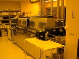
Photolithography
Encyclopedia
Photolithography is a process used in microfabrication
to selectively remove parts of a thin film or the bulk of a substrate
. It uses light to transfer a geometric pattern
from a photomask
to a light-sensitive chemical "photoresist
", or simply "resist," on the substrate. A series of chemical treatments
then either engraves the exposure pattern into, or enables deposition of a new material in the desired pattern upon, the material underneath the photo resist. For example, in complex integrated circuit
s, a modern CMOS
wafer
will go through the photolithographic cycle up to 50 times.
Photolithography shares some fundamental principles with photography
in that the pattern in the etching resist
is created by exposing it to light
, either directly (without using a mask) or with a projected image using an optical mask. This procedure is comparable to a high precision version of the method used to make printed circuit board
s. Subsequent stages in the process have more in common with etching
than with lithographic printing. It is used because it can create extremely small patterns (down to a few tens of nanometers in size), it affords exact control over the shape and size of the objects it creates, and because it can create patterns over an entire surface cost-effectively. Its main disadvantages are that it requires a flat substrate to start with, it is not very effective at creating shapes that are not flat, and it can require extremely clean operating conditions.
ic wafer track systems to coordinate the process. The procedure described here omits some advanced treatments, such as thinning agents or edge-bead removal.
procedure based on solutions containing hydrogen peroxide
.
. A liquid
or gas
eous "adhesion promoter", such as Bis(trimethylsilyl)amine ("hexamethyldisilazane", HMDS)
, is applied to promote adhesion of the photoresist to the wafer. The surface layer of silicon dioxide on the wafer reacts with HMDS to form tri-methylated silicon-dioxide, a highly water repellent layer not unlike the layer of wax on a car's paint. This water repellent layer prevents the aqueous developer from penetrating between the photoresist layer and the wafer's surface, thus preventing so-called lifting of small photoresist structures in the (developing) pattern.
by spin coating. A viscous, liquid solution of photoresist is dispensed onto the wafer, and the wafer is spun rapidly to produce a uniformly thick layer. The spin coating typically runs at 1200 to 4800 rpm for 30 to 60 seconds, and produces a layer between 0.5 and 2.5 micrometres thick. The spin coating process results in a uniform thin layer, usually with uniformity of within 5 to 10 nanometres. This uniformity can be explained by detailed fluid-mechanical modelling, which shows that the resist moves much faster at the top of the layer than at the bottom, where viscous forces bind the resist to the wafer surface. Thus, the top layer of resist is quickly ejected from the wafer's edge while the bottom layer still creeps slowly radially along the wafer. In this way, any 'bump' or 'ridge' of resist is removed, leaving a very flat layer. Final thickness is also determined by the evaporation of liquid solvents from the resist. For very small, dense features (<125 or so nm), thinner resist thicknesses (<0.5 micrometres) are needed to overcome collapse effects at high aspect ratios; typical aspect ratios are <4:1.
The photo resist-coated wafer is then prebaked to drive off excess photoresist solvent, typically at 90 to 100 °C for 30 to 60 seconds on a hotplate.
light (see below). Positive photoresist, the most common type, becomes soluble in the basic developer when exposed; exposed negative photoresist becomes insoluble in the (organic) developer. This chemical change allows some of the photoresist to be removed by a special solution, called "developer" by analogy with photographic developer
. To learn more about the process of exposure and development of positive resist, see, for example: Ralph Dammel, "Diazonaphtoquinone-based resists", SPIE Optical Engineering Press, Vol TT11 (1993).
A PEB (post-exposure bake) is performed before developing, typically to help reduce standing wave
phenomena caused by the destructive and constructive interference patterns of the incident light. In DUV (deep ultraviolet, or shorter than 300 nm exposure wavelength) lithography, CAR (chemically amplified resist) chemistry is used. This process is much more sensitive to PEB time, temperature, and delay, as most of the "exposure" reaction (creating acid, making the polymer soluble in the basic developer) actually occurs in the PEB.
The develop chemistry is delivered on a spinner, much like photoresist. Developers originally often contained sodium hydroxide (NaOH). However, sodium
is considered an extremely undesirable contaminant in MOSFET
fabrication because it degrades the insulating
properties of gate oxides (specifically, sodium ions can migrate in and out of the gate, changing the threshold voltage of the transistor and making it harder or easier to turn the transistor on over time). Metal-ion-free developers such as tetramethylammonium hydroxide
(TMAH) are now used.
The resulting wafer is then "hard-baked" if a non-chemically amplified resist was used, typically at 120 to 180 °C for 20 to 30 minutes. The hard bake solidifies the remaining photoresist, to make a more durable protecting layer in future ion implantation
, wet chemical etching, or plasma etching
.
In etching, a liquid ("wet") or plasma
("dry") chemical agent removes the uppermost layer of the substrate in the areas that are not protected by photoresist. In semiconductor fabrication
, dry etching techniques are generally used, as they can be made anisotropic, in order to avoid significant undercutting of the photoresist pattern. This is essential when the width of the features to be defined is similar to or less than the thickness of the material being etched (i.e. when the aspect ratio approaches unity). Wet etch processes are generally isotropic in nature, which is often indispensable for microelectromechanical systems
, where suspended structures must be "released" from the underlying layer.
The development of low-defectivity anisotropic dry-etch process has enabled the ever-smaller features defined photolithographically in the resist to be transferred to the substrate material.
, which oxidizes it. This process is called ashing
, and resembles dry etching.
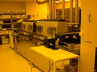 Exposure systems typically produce an image on the wafer using a photomask
. The light shines through the photomask, which blocks it in some areas and lets it pass in others. (Maskless lithography
projects a precise beam directly onto the wafer without using a mask, but it is not widely used in commercial processes.) Exposure systems may be classified by the optics that transfer the image from the mask to the wafer.
Contact printing is liable to damage both the mask and the wafer, and this was the primary reason it was abandoned for high volume production. Both contact and proximity lithography require the light intensity to be uniform across an entire wafer, and the mask to align precisely to features already on the wafer. As modern processes use increasingly large wafers, these conditions become increasingly difficult.
Research and prototyping processes often use contact or proximity lithography, because it uses inexpensive hardware and can achieve high optical resolution. The resolution in proximity lithography is approximately the square root of the product of the wavelength and the gap distance. Hence, except for projection lithography (see below), contact printing offers the best resolution, because its gap distance is approximately zero (neglecting the thickness of the photoresist itself). In addition, nanoimprint lithography may revive interest in this familiar technique, especially since the cost of ownership is expected to be low; however, the shortcomings of contact printing discussed above remain as challenges.
(VLSI) lithography uses projection systems. Unlike contact or proximity masks, which cover an entire wafer, projection masks (known as "reticles") show only one die or an array of die (known as a "field"). Projection exposure systems (steppers or scanners) project the mask onto the wafer many times to create the complete pattern.
The image for the mask originates from a computerized data file. This data file is converted to a series of polygons and written onto a square fused quartz
substrate covered with a layer of chrome
using a photolithographic process. A laser beam (laser writer) or a beam of electrons (e-beam writer) is used to expose the pattern defined by the data file and travels over the surface of the substrate in either a vector or raster scan manner. Where the photoresist on the mask is exposed, the chrome can be etched away, leaving a clear path for the illumination light in the stepper/scanner system to travel through.
 The ability to project a clear image of a small feature onto the wafer is limited by the wavelength
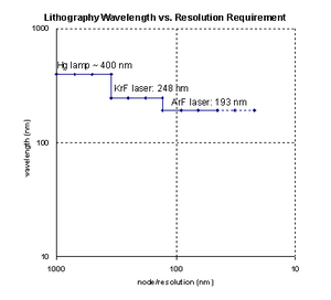
of the light that is used, and the ability of the reduction lens system to capture enough diffraction orders from the illuminated mask. Current state-of-the-art photolithography tools use deep ultraviolet (DUV) light from excimer lasers with wavelengths of 248 and 193 nm
(the dominant lithography technology today is thus also called "excimer laser lithography"), which allow minimum feature sizes down to 50 nm. Excimer laser lithography has thus played a critical role in the continued advance of the so-called Moore’s Law for the last 20 years (see below).
The minimum feature size that a projection system can print is given approximately by:

where
 is the minimum feature size (also called the critical dimension, target design rule). It is also common to write 2 times the half-pitch.
 (commonly called k1 factor) is a coefficient that encapsulates process-related factors, and typically equals 0.4 for production. The minimum feature size can be reduced by decreasing this coefficient through Computational lithography
.
 is the wavelength of light used
 is the numerical aperture
of the lens as seen from the wafer
According to this equation, minimum feature sizes can be decreased by decreasing the wavelength, and increasing the numerical aperture (to achieve a tighter focused beam and a smaller spot size). However, this design method runs into a competing constraint. In modern systems, the depth of focus
is also a concern:

Here, is another process-related coefficient. The depth of focus restricts the thickness of the photoresist and the depth of the topography on the wafer. Chemical mechanical polishing is often used to flatten topography before high-resolution lithographic steps.
 Historically, photolithography has used ultraviolet light from gas-discharge lamp
s using mercury
, sometimes in combination with noble gas
es such as xenon
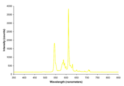
. These lamps produce light across a broad spectrum with several strong peaks in the ultraviolet range. This spectrum is filtered to select a single spectral line
. From the early 1960’s through the mid-1980’s, Hg lamps had been used in lithography for their spectral lines at 436 nm ("g-line"), 405 nm ("h-line") and 365 nm ("i-line"). However, with the semiconductor industry’s need for both higher resolution (to produce denser and faster chips) and higher throughput (for lower costs), the lamp-based lithography tools were no longer able to meet the industry’s requirements.
This challenge was overcome when in a pioneering development in 1982, excimer laser lithography was proposed and demonstrated at I.B.M. by K. Jain, and now excimer laser lithography machines (steppers and scanners) are the primary tools used worldwide in microelectronics production. With phenomenal advances made in tool technology in the last two decades, it is the semiconductor industry view that excimer laser lithography has been a crucial factor in the continued advance of Moore’s Law, enabling minimum features sizes in chip manufacturing to shrink from 0.5 micrometer in 1990 to 45 nanometers and below in 2010. This trend is expected to continue into this decade for even denser chips, with minimum features approaching 10 nanometers. From an even broader scientific and technological perspective, in the 50-year history of the laser since its first demonstration in 1960, the invention and development of excimer laser lithography has been highlighted as one of the major milestones.
The commonly used deep ultraviolet excimer laser
s in lithography systems are the Krypton fluoride laser at 248-nm wavelength and the argon fluoride laser at 193-nm wavelength. The primary manufacturers of excimer laser light sources in the 1980’s were Lambda Physik (now part of Coherent, Inc.) and Lumonics, but since the mid-1990’s Cymer Inc. has become the dominant supplier of excimer laser sources to the lithography equipment manufacturers. Generally, an excimer laser is designed to operate with a specific gas mixture; therefore, changing wavelength is not a trivial matter, as the method of generating the new wavelength is completely different, and the absorption characteristics of materials change. For example, air begins to absorb significantly around the 193 nm wavelength; moving to sub-193 nm wavelengths would require installing vacuum pump and purge equipment on the lithography tools (a significant challenge). Furthermore, insulating materials such as silicon dioxide
(SiO2), when exposed to photons with energy greater than the band gap, release free electrons and holes which subsequently cause adverse charging.
Optical lithography has been extended to feature sizes below 50 nm using the 193 nm ArF excimer laser and liquid immersion techniques. Also termed immersion lithography
, this enables the use of optics with numerical apertures exceeding 1.0. The liquid used is typically ultra-pure, deionised water, which provides for a refractive index
above that of the usual air gap between the lens and the wafer surface. The water is continually circulated to eliminate thermally-induced distortions. Water will only allow NAs of up to ~1.4, but materials with higher refractive indices will allow the effective NA to be increased further.
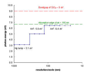 Experimental tools using the 157 nm wavelength from the F2 excimer laser in a manner similar to current exposure systems have been built. These were once targeted to succeed 193 nm lithography at the 65 nm feature size node but have now all but been eliminated by the introduction of immersion lithography. This was due to persistent technical problems with the 157 nm technology and economic considerations that provided strong incentives for the continued use of 193 nm excimer laser lithography technology. High-index immersion lithography is the newest extension of 193 nm lithography to be considered. In 2006, features less than 30 nm were demonstrated by IBM using this technique.
, X-ray lithography
, extreme ultraviolet lithography
and ion projection lithography.
Microfabrication
Microfabrication is the term that describes processes of fabrication of miniature structures, of micrometre sizes and smaller. Historically the earliest microfabrication processes were used for integrated circuit fabrication, also known as "semiconductor manufacturing" or "semiconductor device...
to selectively remove parts of a thin film or the bulk of a substrate
Substrate (printing)
Substrate is a term used in converting process such as printing and Lamination or coating as a more general term to describe the base material onto which e.g. images will be printed and to be laminated as per the packing specification required for the product...
. It uses light to transfer a geometric pattern
Geometry
Geometry arose as the field of knowledge dealing with spatial relationships. Geometry was one of the two fields of pre-modern mathematics, the other being the study of numbers ....
from a photomask
Photomask
A photomask is an opaque plate with holes or transparencies that allow light to shine through in a defined pattern. They are commonly used in photolithography.-Overview:...
to a light-sensitive chemical "photoresist
Photoresist
A photoresist is a light-sensitive material used in several industrial processes, such as photolithography and photoengraving to form a patterned coating on a surface.-Tone:Photoresists are classified into two groups: positive resists and negative resists....
", or simply "resist," on the substrate. A series of chemical treatments
Chemical engineering
Chemical engineering is the branch of engineering that deals with physical science , and life sciences with mathematics and economics, to the process of converting raw materials or chemicals into more useful or valuable forms...
then either engraves the exposure pattern into, or enables deposition of a new material in the desired pattern upon, the material underneath the photo resist. For example, in complex integrated circuit
Integrated circuit
An integrated circuit or monolithic integrated circuit is an electronic circuit manufactured by the patterned diffusion of trace elements into the surface of a thin substrate of semiconductor material...
s, a modern CMOS
CMOS
Complementary metal–oxide–semiconductor is a technology for constructing integrated circuits. CMOS technology is used in microprocessors, microcontrollers, static RAM, and other digital logic circuits...
wafer
Wafer (electronics)
A wafer is a thin slice of semiconductor material, such as a silicon crystal, used in the fabrication of integrated circuits and other microdevices...
will go through the photolithographic cycle up to 50 times.
Photolithography shares some fundamental principles with photography
Photography
Photography is the art, science and practice of creating durable images by recording light or other electromagnetic radiation, either electronically by means of an image sensor or chemically by means of a light-sensitive material such as photographic film...
in that the pattern in the etching resist
Resist
In semiconductor fabrication, a resist is a thin layer used to transfer a circuit pattern to the semiconductor substrate which it is deposited upon. A resist can be patterned via lithography to form a micrometer-scale, temporary mask that protects selected areas of the underlying substrate during...
is created by exposing it to light
Light
Light or visible light is electromagnetic radiation that is visible to the human eye, and is responsible for the sense of sight. Visible light has wavelength in a range from about 380 nanometres to about 740 nm, with a frequency range of about 405 THz to 790 THz...
, either directly (without using a mask) or with a projected image using an optical mask. This procedure is comparable to a high precision version of the method used to make printed circuit board
Printed circuit board
A printed circuit board, or PCB, is used to mechanically support and electrically connect electronic components using conductive pathways, tracks or signal traces etched from copper sheets laminated onto a non-conductive substrate. It is also referred to as printed wiring board or etched wiring...
s. Subsequent stages in the process have more in common with etching
Etching
Etching is the process of using strong acid or mordant to cut into the unprotected parts of a metal surface to create a design in intaglio in the metal...
than with lithographic printing. It is used because it can create extremely small patterns (down to a few tens of nanometers in size), it affords exact control over the shape and size of the objects it creates, and because it can create patterns over an entire surface cost-effectively. Its main disadvantages are that it requires a flat substrate to start with, it is not very effective at creating shapes that are not flat, and it can require extremely clean operating conditions.
Basic procedure
A single iteration of photolithography combines several steps in sequence. Modern cleanrooms use automated, robotIndustrial robot
An industrial robot is defined by ISO as an automatically controlled, reprogrammable, multipurpose manipulator programmable in three or more axes...
ic wafer track systems to coordinate the process. The procedure described here omits some advanced treatments, such as thinning agents or edge-bead removal.
Cleaning
If organic or inorganic contaminations are present on the wafer surface, they are usually removed by wet chemical treatment, e.g. the RCA cleanRCA clean
The RCA clean is a standard set of wafer cleaning steps which needs to be performed before high temp processing steps of silicon wafers in semiconductor manufacturing. RCA cleaning includes RCA-1 and RCA-2 cleaning procedures...
procedure based on solutions containing hydrogen peroxide
Hydrogen peroxide
Hydrogen peroxide is the simplest peroxide and an oxidizer. Hydrogen peroxide is a clear liquid, slightly more viscous than water. In dilute solution, it appears colorless. With its oxidizing properties, hydrogen peroxide is often used as a bleach or cleaning agent...
.
Preparation
The wafer is initially heated to a temperature sufficient to drive off any moisture that may be present on the wafer surface. Wafers that have been in storage must be chemically cleaned to remove contaminationContamination
Contamination is the presence of a minor and unwanted constituent in material, physical body, natural environment, at a workplace, etc.-Specifics:"Contamination" also has more specific meanings in science:...
. A liquid
Liquid
Liquid is one of the three classical states of matter . Like a gas, a liquid is able to flow and take the shape of a container. Some liquids resist compression, while others can be compressed. Unlike a gas, a liquid does not disperse to fill every space of a container, and maintains a fairly...
or gas
Gas
Gas is one of the three classical states of matter . Near absolute zero, a substance exists as a solid. As heat is added to this substance it melts into a liquid at its melting point , boils into a gas at its boiling point, and if heated high enough would enter a plasma state in which the electrons...
eous "adhesion promoter", such as Bis(trimethylsilyl)amine ("hexamethyldisilazane", HMDS)
Bis(trimethylsilyl)amine
Bisamine is an organosilicon compound with the molecular formula [3Si]2NH. The molecule is a derivative of ammonia with trimethylsilyl groups in place of two hydrogen atoms...
, is applied to promote adhesion of the photoresist to the wafer. The surface layer of silicon dioxide on the wafer reacts with HMDS to form tri-methylated silicon-dioxide, a highly water repellent layer not unlike the layer of wax on a car's paint. This water repellent layer prevents the aqueous developer from penetrating between the photoresist layer and the wafer's surface, thus preventing so-called lifting of small photoresist structures in the (developing) pattern.
Photoresist application
The wafer is covered with photoresistPhotoresist
A photoresist is a light-sensitive material used in several industrial processes, such as photolithography and photoengraving to form a patterned coating on a surface.-Tone:Photoresists are classified into two groups: positive resists and negative resists....
by spin coating. A viscous, liquid solution of photoresist is dispensed onto the wafer, and the wafer is spun rapidly to produce a uniformly thick layer. The spin coating typically runs at 1200 to 4800 rpm for 30 to 60 seconds, and produces a layer between 0.5 and 2.5 micrometres thick. The spin coating process results in a uniform thin layer, usually with uniformity of within 5 to 10 nanometres. This uniformity can be explained by detailed fluid-mechanical modelling, which shows that the resist moves much faster at the top of the layer than at the bottom, where viscous forces bind the resist to the wafer surface. Thus, the top layer of resist is quickly ejected from the wafer's edge while the bottom layer still creeps slowly radially along the wafer. In this way, any 'bump' or 'ridge' of resist is removed, leaving a very flat layer. Final thickness is also determined by the evaporation of liquid solvents from the resist. For very small, dense features (<125 or so nm), thinner resist thicknesses (<0.5 micrometres) are needed to overcome collapse effects at high aspect ratios; typical aspect ratios are <4:1.
The photo resist-coated wafer is then prebaked to drive off excess photoresist solvent, typically at 90 to 100 °C for 30 to 60 seconds on a hotplate.
Exposure and developing
After prebaking, the photoresist is exposed to a pattern of intense light. Optical lithography typically uses ultravioletUltraviolet
Ultraviolet light is electromagnetic radiation with a wavelength shorter than that of visible light, but longer than X-rays, in the range 10 nm to 400 nm, and energies from 3 eV to 124 eV...
light (see below). Positive photoresist, the most common type, becomes soluble in the basic developer when exposed; exposed negative photoresist becomes insoluble in the (organic) developer. This chemical change allows some of the photoresist to be removed by a special solution, called "developer" by analogy with photographic developer
Photographic developer
In the processing of photographic films, plates or papers, the photographic developer is a chemical that makes the latent image on the film or print visible. It does this by reducing the silver halides that have been exposed to light to elemental silver in the gelatine matrix...
. To learn more about the process of exposure and development of positive resist, see, for example: Ralph Dammel, "Diazonaphtoquinone-based resists", SPIE Optical Engineering Press, Vol TT11 (1993).
A PEB (post-exposure bake) is performed before developing, typically to help reduce standing wave
Standing wave
In physics, a standing wave – also known as a stationary wave – is a wave that remains in a constant position.This phenomenon can occur because the medium is moving in the opposite direction to the wave, or it can arise in a stationary medium as a result of interference between two waves traveling...
phenomena caused by the destructive and constructive interference patterns of the incident light. In DUV (deep ultraviolet, or shorter than 300 nm exposure wavelength) lithography, CAR (chemically amplified resist) chemistry is used. This process is much more sensitive to PEB time, temperature, and delay, as most of the "exposure" reaction (creating acid, making the polymer soluble in the basic developer) actually occurs in the PEB.
The develop chemistry is delivered on a spinner, much like photoresist. Developers originally often contained sodium hydroxide (NaOH). However, sodium
Sodium
Sodium is a chemical element with the symbol Na and atomic number 11. It is a soft, silvery-white, highly reactive metal and is a member of the alkali metals; its only stable isotope is 23Na. It is an abundant element that exists in numerous minerals, most commonly as sodium chloride...
is considered an extremely undesirable contaminant in MOSFET
MOSFET
The metal–oxide–semiconductor field-effect transistor is a transistor used for amplifying or switching electronic signals. The basic principle of this kind of transistor was first patented by Julius Edgar Lilienfeld in 1925...
fabrication because it degrades the insulating
Electrical insulation
thumb|250px|[[Coaxial Cable]] with dielectric insulator supporting a central coreThis article refers to electrical insulation. For insulation of heat, see Thermal insulation...
properties of gate oxides (specifically, sodium ions can migrate in and out of the gate, changing the threshold voltage of the transistor and making it harder or easier to turn the transistor on over time). Metal-ion-free developers such as tetramethylammonium hydroxide
Tetramethylammonium hydroxide
Tetramethylammonium hydroxide is a quaternary ammonium salt with the molecular formula 4NOH. It is used as an anisotropic etchant of silicon. It is also used as a basic solvent in the development of acidic photoresist in the photolithography process. Since it is a phase transfer catalyst, it is...
(TMAH) are now used.
The resulting wafer is then "hard-baked" if a non-chemically amplified resist was used, typically at 120 to 180 °C for 20 to 30 minutes. The hard bake solidifies the remaining photoresist, to make a more durable protecting layer in future ion implantation
Ion implantation
Ion implantation is a materials engineering process by which ions of a material are accelerated in an electrical field and impacted into another solid. This process is used to change the physical, chemical, or electrical properties of the solid...
, wet chemical etching, or plasma etching
Plasma etching
Plasma etching is a form of plasma processing used to fabricate integrated circuits. It involves a high-speed stream of glow discharge of an appropriate gas mixture being shot at a sample. The plasma source, known as etch species, can be either charged or neutral...
.
Etching
In etching, a liquid ("wet") or plasma
Plasma (physics)
In physics and chemistry, plasma is a state of matter similar to gas in which a certain portion of the particles are ionized. Heating a gas may ionize its molecules or atoms , thus turning it into a plasma, which contains charged particles: positive ions and negative electrons or ions...
("dry") chemical agent removes the uppermost layer of the substrate in the areas that are not protected by photoresist. In semiconductor fabrication
Semiconductor fabrication
Semiconductor device fabrication is the process used to create the integrated circuits that are present in everyday electrical and electronic devices. It is a multiple-step sequence of photolithographic and chemical processing steps during which electronic circuits are gradually created on a wafer...
, dry etching techniques are generally used, as they can be made anisotropic, in order to avoid significant undercutting of the photoresist pattern. This is essential when the width of the features to be defined is similar to or less than the thickness of the material being etched (i.e. when the aspect ratio approaches unity). Wet etch processes are generally isotropic in nature, which is often indispensable for microelectromechanical systems
Microelectromechanical systems
Microelectromechanical systems is the technology of very small mechanical devices driven by electricity; it merges at the nano-scale into nanoelectromechanical systems and nanotechnology...
, where suspended structures must be "released" from the underlying layer.
The development of low-defectivity anisotropic dry-etch process has enabled the ever-smaller features defined photolithographically in the resist to be transferred to the substrate material.
Photoresist removal
After a photoresist is no longer needed, it must be removed from the substrate. This usually requires a liquid "resist stripper", which chemically alters the resist so that it no longer adheres to the substrate. Alternatively, photoresist may be removed by a plasma containing oxygenOxygen
Oxygen is the element with atomic number 8 and represented by the symbol O. Its name derives from the Greek roots ὀξύς and -γενής , because at the time of naming, it was mistakenly thought that all acids required oxygen in their composition...
, which oxidizes it. This process is called ashing
Plasma ashing
In semiconductor manufacturing plasma ashing is the process of removing the photoresist from an etched wafer. Using a plasma source, a monatomic reactive species is generated. Oxygen or fluorine are the most common reactive species...
, and resembles dry etching.
Exposure ("printing") systems

Photomask
A photomask is an opaque plate with holes or transparencies that allow light to shine through in a defined pattern. They are commonly used in photolithography.-Overview:...
. The light shines through the photomask, which blocks it in some areas and lets it pass in others. (Maskless lithography
Maskless lithography
In maskless lithography, the radiation that is used to expose a photosensitive emulsion is not projected from, or transmitted through, a photomask. Instead, most commonly, the radiation is focused to a narrow beam. The beam is then used to directly write the image into the photoresist, one or more...
projects a precise beam directly onto the wafer without using a mask, but it is not widely used in commercial processes.) Exposure systems may be classified by the optics that transfer the image from the mask to the wafer.
Contact and proximity
A contact printer, the simplest exposure system, puts a photomask in direct contact with the wafer and exposes it to a uniform light. A proximity printer puts a small gap between the photomask and wafer. In both cases, the mask covers the entire wafer, and simultaneously patterns every die.Contact printing is liable to damage both the mask and the wafer, and this was the primary reason it was abandoned for high volume production. Both contact and proximity lithography require the light intensity to be uniform across an entire wafer, and the mask to align precisely to features already on the wafer. As modern processes use increasingly large wafers, these conditions become increasingly difficult.
Research and prototyping processes often use contact or proximity lithography, because it uses inexpensive hardware and can achieve high optical resolution. The resolution in proximity lithography is approximately the square root of the product of the wavelength and the gap distance. Hence, except for projection lithography (see below), contact printing offers the best resolution, because its gap distance is approximately zero (neglecting the thickness of the photoresist itself). In addition, nanoimprint lithography may revive interest in this familiar technique, especially since the cost of ownership is expected to be low; however, the shortcomings of contact printing discussed above remain as challenges.
Projection
Very-large-scale integrationVery-large-scale integration
Very-large-scale integration is the process of creating integrated circuits by combining thousands of transistors into a single chip. VLSI began in the 1970s when complex semiconductor and communication technologies were being developed. The microprocessor is a VLSI device.The first semiconductor...
(VLSI) lithography uses projection systems. Unlike contact or proximity masks, which cover an entire wafer, projection masks (known as "reticles") show only one die or an array of die (known as a "field"). Projection exposure systems (steppers or scanners) project the mask onto the wafer many times to create the complete pattern.
Photomasks
The image for the mask originates from a computerized data file. This data file is converted to a series of polygons and written onto a square fused quartz
Fused quartz
Fused quartz and fused silica are types of glass containing primarily silica in amorphous form. They are manufactured using several different processes...
substrate covered with a layer of chrome
Chromium
Chromium is a chemical element which has the symbol Cr and atomic number 24. It is the first element in Group 6. It is a steely-gray, lustrous, hard metal that takes a high polish and has a high melting point. It is also odorless, tasteless, and malleable...
using a photolithographic process. A laser beam (laser writer) or a beam of electrons (e-beam writer) is used to expose the pattern defined by the data file and travels over the surface of the substrate in either a vector or raster scan manner. Where the photoresist on the mask is exposed, the chrome can be etched away, leaving a clear path for the illumination light in the stepper/scanner system to travel through.
Resolution in projection systems

Wavelength
In physics, the wavelength of a sinusoidal wave is the spatial period of the wave—the distance over which the wave's shape repeats.It is usually determined by considering the distance between consecutive corresponding points of the same phase, such as crests, troughs, or zero crossings, and is a...
of the light that is used, and the ability of the reduction lens system to capture enough diffraction orders from the illuminated mask. Current state-of-the-art photolithography tools use deep ultraviolet (DUV) light from excimer lasers with wavelengths of 248 and 193 nm
Nanometre
A nanometre is a unit of length in the metric system, equal to one billionth of a metre. The name combines the SI prefix nano- with the parent unit name metre .The nanometre is often used to express dimensions on the atomic scale: the diameter...
(the dominant lithography technology today is thus also called "excimer laser lithography"), which allow minimum feature sizes down to 50 nm. Excimer laser lithography has thus played a critical role in the continued advance of the so-called Moore’s Law for the last 20 years (see below).
The minimum feature size that a projection system can print is given approximately by:

where
 is the minimum feature size (also called the critical dimension, target design rule). It is also common to write 2 times the half-pitch.
 (commonly called k1 factor) is a coefficient that encapsulates process-related factors, and typically equals 0.4 for production. The minimum feature size can be reduced by decreasing this coefficient through Computational lithography
Computational lithography
Computational lithography is the set of mathematical and algorithmic approaches designed to improve the resolution attainable through photolithography...
.
 is the wavelength of light used
 is the numerical aperture
Numerical aperture
In optics, the numerical aperture of an optical system is a dimensionless number that characterizes the range of angles over which the system can accept or emit light. By incorporating index of refraction in its definition, NA has the property that it is constant for a beam as it goes from one...
of the lens as seen from the wafer
According to this equation, minimum feature sizes can be decreased by decreasing the wavelength, and increasing the numerical aperture (to achieve a tighter focused beam and a smaller spot size). However, this design method runs into a competing constraint. In modern systems, the depth of focus
Depth of focus
Depth of focus is a lens optics concept that measures the tolerance of placement of the image plane in relation to the lens...
is also a concern:

Here,
 is another process-related coefficient. The depth of focus restricts the thickness of the photoresist and the depth of the topography on the wafer. Chemical mechanical polishing is often used to flatten topography before high-resolution lithographic steps.
Light sources

Gas-discharge lamp
Gas-discharge lamps are a family of artificial light sources that generate light by sending an electrical discharge through an ionized gas, i.e. a plasma. The character of the gas discharge critically depends on the frequency or modulation of the current: see the entry on a frequency classification...
s using mercury
Mercury (element)
Mercury is a chemical element with the symbol Hg and atomic number 80. It is also known as quicksilver or hydrargyrum...
, sometimes in combination with noble gas
Noble gas
The noble gases are a group of chemical elements with very similar properties: under standard conditions, they are all odorless, colorless, monatomic gases, with very low chemical reactivity...
es such as xenon
Xenon
Xenon is a chemical element with the symbol Xe and atomic number 54. The element name is pronounced or . A colorless, heavy, odorless noble gas, xenon occurs in the Earth's atmosphere in trace amounts...
. These lamps produce light across a broad spectrum with several strong peaks in the ultraviolet range. This spectrum is filtered to select a single spectral line
Spectral line
A spectral line is a dark or bright line in an otherwise uniform and continuous spectrum, resulting from a deficiency or excess of photons in a narrow frequency range, compared with the nearby frequencies.- Types of line spectra :...
. From the early 1960’s through the mid-1980’s, Hg lamps had been used in lithography for their spectral lines at 436 nm ("g-line"), 405 nm ("h-line") and 365 nm ("i-line"). However, with the semiconductor industry’s need for both higher resolution (to produce denser and faster chips) and higher throughput (for lower costs), the lamp-based lithography tools were no longer able to meet the industry’s requirements.
This challenge was overcome when in a pioneering development in 1982, excimer laser lithography was proposed and demonstrated at I.B.M. by K. Jain, and now excimer laser lithography machines (steppers and scanners) are the primary tools used worldwide in microelectronics production. With phenomenal advances made in tool technology in the last two decades, it is the semiconductor industry view that excimer laser lithography has been a crucial factor in the continued advance of Moore’s Law, enabling minimum features sizes in chip manufacturing to shrink from 0.5 micrometer in 1990 to 45 nanometers and below in 2010. This trend is expected to continue into this decade for even denser chips, with minimum features approaching 10 nanometers. From an even broader scientific and technological perspective, in the 50-year history of the laser since its first demonstration in 1960, the invention and development of excimer laser lithography has been highlighted as one of the major milestones.
The commonly used deep ultraviolet excimer laser
Excimer laser
An excimer laser is a form of ultraviolet laser which is commonly used in the production of microelectronic devices , eye surgery, and micromachining....
s in lithography systems are the Krypton fluoride laser at 248-nm wavelength and the argon fluoride laser at 193-nm wavelength. The primary manufacturers of excimer laser light sources in the 1980’s were Lambda Physik (now part of Coherent, Inc.) and Lumonics, but since the mid-1990’s Cymer Inc. has become the dominant supplier of excimer laser sources to the lithography equipment manufacturers. Generally, an excimer laser is designed to operate with a specific gas mixture; therefore, changing wavelength is not a trivial matter, as the method of generating the new wavelength is completely different, and the absorption characteristics of materials change. For example, air begins to absorb significantly around the 193 nm wavelength; moving to sub-193 nm wavelengths would require installing vacuum pump and purge equipment on the lithography tools (a significant challenge). Furthermore, insulating materials such as silicon dioxide
Silicon dioxide
The chemical compound silicon dioxide, also known as silica , is an oxide of silicon with the chemical formula '. It has been known for its hardness since antiquity...
(SiO2), when exposed to photons with energy greater than the band gap, release free electrons and holes which subsequently cause adverse charging.
Optical lithography has been extended to feature sizes below 50 nm using the 193 nm ArF excimer laser and liquid immersion techniques. Also termed immersion lithography
Immersion lithography
Immersion lithography is a photolithography resolution enhancement technique for manufacturing integrated circuits that replaces the usual air gap between the final lens and the wafer surface with a liquid medium that has a refractive index greater than one. The resolution is increased by a factor...
, this enables the use of optics with numerical apertures exceeding 1.0. The liquid used is typically ultra-pure, deionised water, which provides for a refractive index
Refractive index
In optics the refractive index or index of refraction of a substance or medium is a measure of the speed of light in that medium. It is expressed as a ratio of the speed of light in vacuum relative to that in the considered medium....
above that of the usual air gap between the lens and the wafer surface. The water is continually circulated to eliminate thermally-induced distortions. Water will only allow NAs of up to ~1.4, but materials with higher refractive indices will allow the effective NA to be increased further.

Experimental methods
Photolithography has been defeating predictions of its demise for many years. For instance, by the early 1980s, many in the semiconductor industry had come to believe that features smaller than 1 micrometer could not be printed optically. Modern techniques using excimer laser lithography already print features with dimensions a fraction of the wavelength of light used - an amazing optical feat. New tricks such as immersion lithography, dual-tone resist and multiple patterning continue to improve the resolution of 193nm lithography. Meanwhile, current research is exploring alternatives to conventional UV, such as electron beam lithographyElectron beam lithography
Electron beam lithography is the practice of emitting a beam of electrons in a patterned fashion across a surface covered with a film , and of selectively removing either exposed or non-exposed regions of the resist...
, X-ray lithography
X-ray lithography
300px|thumbX-ray lithography, is a process used in electronic industry to selectively remove parts of a thin film. It uses X-rays to transfer a geometric pattern from a mask to a light-sensitive chemical photoresist, or simply "resist," on the substrate...
, extreme ultraviolet lithography
Extreme ultraviolet lithography
Extreme ultraviolet lithography is a next-generation lithography technology using an extreme ultraviolet wavelength, currently expected to be 13.5 nm.-EUVL light source:...
and ion projection lithography.
See also
- Alternative types of lithography
- Nanoimprint lithographyNanoimprint LithographyNanoimprint lithography is a method of fabricating nanometer scale patterns. It is a simple nanolithography process with low cost, high throughput and high resolution. It creates patterns by mechanical deformation of imprint resist and subsequent processes. The imprint resist is typically a monomer...
- Dip-pen nanolithography
- Soft lithographySoft lithography200px|right|thumb|Figure 1 - "Inking" a stamp. PDMS stamp with pattern is placed in Ethanol and ODT solution200px|right|thumb|Figure 2 - ODT from the solution settles down onto the PDMS stamp. Stamp now has ODT attached to it which acts as the ink....
- MagnetolithographyMagnetolithographyMagnetolithography is a method for pattern surfaces. ML based on applying a magnetic field on the substrate using paramagnetic metal masks named "magnetic mask". Magnetic mask which is analog to photomask define the spatial distribution and shape of the applied magnetic field...
- Nanochannel glass materialsNanochannel glass materialsNanochannel glass materials are an experimental mask technology that is an alternate method for fabricating nanostructures, although optical lithography is the predominant patterning technique....
- Nanoimprint lithography
- Excimer lasers
- Moore's lawMoore's LawMoore's law describes a long-term trend in the history of computing hardware: the number of transistors that can be placed inexpensively on an integrated circuit doubles approximately every two years....
- Computational lithographyComputational lithographyComputational lithography is the set of mathematical and algorithmic approaches designed to improve the resolution attainable through photolithography...
- StereolithographyStereolithographyStereolithography is an additive manufacturing technology for producing models, prototypes, patterns, and in some cases, production parts.-Technology description:...
, a macroscale process used to produce three-dimensional shapes - Wafer foundry
External links
- BYU Photolithography Resources
- Semiconductor Lithography — Overview of lithography
- Optical Lithography Introduction — IBM site with lithography-related articles
- Immersion Lithography Article — Shows how depth-of-focus is increased with immersion lithography
- Photolithography Equipment- UV Light Shields & Information
- Photo Etching Experts

