
Kikuchi line
Encyclopedia
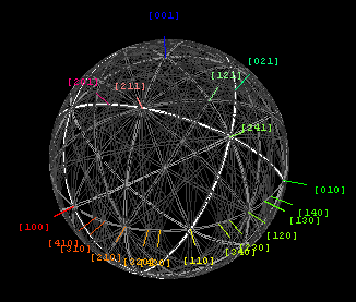
Electron diffraction
Electron diffraction refers to the wave nature of electrons. However, from a technical or practical point of view, it may be regarded as a technique used to study matter by firing electrons at a sample and observing the resulting interference pattern...
from single crystal specimens, there to serve as "roads in orientation-space" for microscopists not sure what they are looking at. In transmission electron microscopes, they are easily seen in diffraction from regions of the specimen thick enough for multiple scattering. Unlike diffraction spots, which blink on and off as one tilts the crystal, Kikuchi bands mark orientation space with well-defined intersections (called zones or poles) as well as paths connecting one intersection to the next.
Experimental and theoretical maps of Kikuchi band geometry, as well as their direct-space analogs e.g. bend contours, electron channeling patterns, and fringe visibility maps are increasingly useful tools in electron microscopy of crystal
Crystal
A crystal or crystalline solid is a solid material whose constituent atoms, molecules, or ions are arranged in an orderly repeating pattern extending in all three spatial dimensions. The scientific study of crystals and crystal formation is known as crystallography...
line and nanocrystal
Nanocrystal
B. D. Fahlman has described a nanocrystal as any nanomaterial with at least one dimension ≤ 100nm and that is singlecrystalline.-Summary:More properly, any material with a dimension of less than 1 micrometre, i.e., 1000 nanometers, should be referred to as a nanoparticle, not a nanocrystal...
line materials. Because each Kikuchi line is associated with Bragg diffraction from one side of a single set of lattice planes, these lines can be labeled with the same Miller
Miller index
Miller indices form a notation system in crystallography for planes and directions in crystal lattices.In particular, a family of lattice planes is determined by three integers h, k, and ℓ, the Miller indices. They are written , and each index denotes a plane orthogonal to a direction in the...
or reciprocal-lattice
Reciprocal lattice
In physics, the reciprocal lattice of a lattice is the lattice in which the Fourier transform of the spatial function of the original lattice is represented. This space is also known as momentum space or less commonly k-space, due to the relationship between the Pontryagin duals momentum and...
indices that are used to identify individual diffraction spots. Kikuchi band intersections, or zones, on the other hand are indexed with direct-lattice indices i.e. indices which represent integer multiples of the lattice basis vectors a, b and c.
Kikuchi lines are formed in diffraction patterns by diffusely scattered electrons, e.g. as a result of thermal atom vibrations. The main features of their geometry can be deduced from a simple elastic mechanism proposed in 1928 by Seishi Kikuchi
Seishi Kikuchi
was a Japanese physicist, known for his explanation of the Kikuchi lines that show up in diffraction patterns of diffusely scattered electrons.-Biography:Seishi Kikuchi was born and grew up in Tokyo. He graduated in 1926 from Tokyo Imperial University....
, although the dynamical theory of diffuse inelastic scattering
Inelastic scattering
In particle physics and chemistry, inelastic scattering is a fundamental scattering process in which the kinetic energy of an incident particle is not conserved . In an inelastic scattering process, some of the energy of the incident particle is lost or gained...
is needed to understand them quantitatively.
In x-ray scattering these lines are referred to as Kossel lines (named after Walther Kossel
Walther Kossel
Walther Ludwig Julius Kossel was a German physicist known for his theory of the chemical bond , Sommerfeld–Kossel displacement law of atomic spectra, the Kossel-Stranski model for crystal growth, and the Kossel effect...
).
Recording experimental Kikuchi patterns and maps
Silicon
Silicon is a chemical element with the symbol Si and atomic number 14. A tetravalent metalloid, it is less reactive than its chemical analog carbon, the nonmetal directly above it in the periodic table, but more reactive than germanium, the metalloid directly below it in the table...
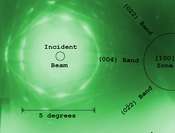
[100] zone, taken with the beam direction approximately 7.9° away from the zone along the (004) Kikuchi band. The dynamic range
Dynamic range
Dynamic range, abbreviated DR or DNR, is the ratio between the largest and smallest possible values of a changeable quantity, such as in sound and light. It is measured as a ratio, or as a base-10 or base-2 logarithmic value.-Dynamic range and human perception:The human senses of sight and...
in the image is so large that only portions of the film are not overexposed
Exposure (photography)
In photography, exposure is the total amount of light allowed to fall on the photographic medium during the process of taking a photograph. Exposure is measured in lux seconds, and can be computed from exposure value and scene luminance over a specified area.In photographic jargon, an exposure...
. Kikuchi lines are much easier to follow with dark-adapted eyes on a fluorescent screen, than they are to capture unmoving on paper or film, even though eye
Human eye
The human eye is an organ which reacts to light for several purposes. As a conscious sense organ, the eye allows vision. Rod and cone cells in the retina allow conscious light perception and vision including color differentiation and the perception of depth...
s and photographic media
Photographic film
Photographic film is a sheet of plastic coated with an emulsion containing light-sensitive silver halide salts with variable crystal sizes that determine the sensitivity, contrast and resolution of the film...
both have a roughly logarithmic
Logarithmic scale
A logarithmic scale is a scale of measurement using the logarithm of a physical quantity instead of the quantity itself.A simple example is a chart whose vertical axis increments are labeled 1, 10, 100, 1000, instead of 1, 2, 3, 4...
response to illumination intensity. Fully quantitative work on such diffraction features is therefore assisted by the large linear dynamic range of CCD detectors
Charge-coupled device
A charge-coupled device is a device for the movement of electrical charge, usually from within the device to an area where the charge can be manipulated, for example conversion into a digital value. This is achieved by "shifting" the signals between stages within the device one at a time...
.
This image subtends an angular range of over 10° and required use of a shorter than usual camera length L. The Kikuchi band widths themselves (roughly λL/d where λ/d is approximately twice the Bragg angle
Bragg's law
In physics, Bragg's law gives the angles for coherent and incoherent scattering from a crystal lattice. When X-rays are incident on an atom, they make the electronic cloud move as does any electromagnetic wave...
for the corresponding plane) are well under 1°, because the wavelength λ of electrons (about 1.97 picometres in this case) is much less than the lattice plane d-spacing itself. For comparison, the d-spacing for silicon (022) is about 192 picometres while the d-spacing for silicon (004) is about 136 picometres.
The image was taken from a region of the crystal which is thicker than the inelastic mean free path
Inelastic mean free path
The inelastic mean free path is an index of how far an electron can travel through a solid before losing energy.If a monochromatic primary beam of electrons is incident on a solid surface, the majority of incident electrons lose their energy because they interact strongly with matter, leading to...
(about 200 nanometres), so that diffuse scattering features (the Kikuchi lines) would be strong in comparison to coherent scattering features (diffraction spots). The fact that surviving diffraction spots appear as disks intersected by bright Kikuchi lines means that the diffraction pattern was taken with a convergent electron beam. In practice, Kikuchi lines are easily seen in thick regions of either selected area
Selected area diffraction
Selected area diffraction , is a crystallographic experimental technique that can be performed inside a transmission electron microscope ....
or convergent beam electron diffraction
Electron diffraction
Electron diffraction refers to the wave nature of electrons. However, from a technical or practical point of view, it may be regarded as a technique used to study matter by firing electrons at a sample and observing the resulting interference pattern...
patterns, but difficult to see in diffraction from crystals much less than 100 nm in size (where lattice-fringe visibility effects become important instead). This image was recorded in convergent beam, because that too reduces the range of contrasts that have to be recorded on film.
Compiling Kikuchi maps which cover more than a steradian
Steradian
The steradian is the SI unit of solid angle. It is used to describe two-dimensional angular spans in three-dimensional space, analogous to the way in which the radian describes angles in a plane...
requires that one take many images at tilts changed only incrementally (e.g. by 2° in each direction). This can be tedious work, but may be useful when investigating a crystal with unknown structure as it can clearly unveil the lattice symmetry in three dimensions.
Kikuchi line maps and their stereographic projection
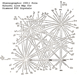
Note also that the figure at left is excerpted from a stereographic projection
Stereographic projection
The stereographic projection, in geometry, is a particular mapping that projects a sphere onto a plane. The projection is defined on the entire sphere, except at one point — the projection point. Where it is defined, the mapping is smooth and bijective. It is conformal, meaning that it...
centered on that [001] zone. Such conformal projections allow one to map pieces of spherical surface onto a plane while preserving the local angles of intersection, and hence zone symmetries. Plotting such maps requires that one be able to draw arcs of circles with a very large radius of curvature. The figure at left, for example, was drawn before the advent of computers and hence required the use of a beam compass. Finding a beam compass today might be fairly difficult, since it is much easier to draw curves having a large radius of curvature (in two or three dimensions) with help from a computer.
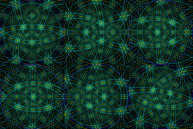
The angle-preserving effect of stereographic plots is even more obvious in the figure at right, which subtends a full 180° of the orientation space of a face-centered or cubic close packed crystal e.g. like that of Gold or Aluminum. The animation follows {220} fringe-visibility bands of that face-centered cubic crystal between <111> zones, at which point rotation by 60° sets up travel to the next <111> zone via a repeat of the original sequence. Fringe-visibility bands have the same global geometry as do Kikuchi bands, but for thin specimens their width is proportional (rather than inversely proportional) to d-spacing. Although the angular field width (and tilt range) obtainable experimentally with Kikuchi bands is generally much smaller, the animation offers a wide-angle view of how Kikuchi bands help informed crystallographers find their way between landmarks in the orientation space of a single crystal specimen.
Real space analogs
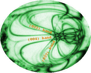
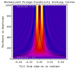
Bend contours and rocking curves
The [100] bend contour "spider" of this image, trapped in a region of silicon that was shaped like an oval watchglass less than a micrometre in size, was imaged with 300 keV electrons. If you tilt the crystal, the spider moves toward the edges of the oval as though it is trying to get out. For example, in this image the spider's [100] intersection has moved to the right side of the ellipse as the specimen was tilted to the left.
The spider's legs, and their intersections, can be indexed as shown in precisely the same way as the Kikuchi pattern near [100] in the section on experimental Kikuchi patterns above. In principle, one could therefore use this bend contour to model the foil's vector tilt (with milliradian accuracy) at all points across the oval.
Lattice fringe visibility maps
As you can see from the rocking curve above, as specimen thickness moves into the 10 nanometre and smaller range (e.g. for 300 keV electrons and lattice spacings near 0.23 nm) the angular range of tilts that give rise to diffraction and/or lattice-fringe contrast becomes inversely proportional to specimen thickness. The geometry of lattice-fringe visibility therefore becomes useful in the electron microscope study of nanomaterials, just as bend contours and Kikuchi lines are useful in the study of single crystal specimens (e.g. metals and semiconductor specimens with thickness in the tenth-micrometre range). Applications to nanostructure for example include: (i) determining the 3D lattice parameters of individual nanoparticles from images taken at different tilts, (ii) fringe fingerprinting of randomly-oriented nanoparticle collections, (iii) particle thickness maps based on fringe contrast changes under tilt, (iv) detection of icosahedral twinning from the lattice image of a randomly-oriented nanoparticle, and (v) analysis of orientation relationships between nanoparticles and a cylindrical support.Electron channeling patterns
The above techniques all involve detection of electrons which have passed through a thin specimen, usually in a transmission electron microscope. Scanning electron microscopeScanning electron microscope
A scanning electron microscope is a type of electron microscope that images a sample by scanning it with a high-energy beam of electrons in a raster scan pattern...
s, on the other hand, typically look at electrons "kicked up" when one rasters a focussed electron beam across a thick specimen. Electron channeling patterns are contrast effects associated with edge-on lattice planes that show up in scanning electron microscope secondary and/or backscattered electron images.
The contrast effects are to first order similar to those of bend contours, i.e. electrons which enter a crystalline surface under diffracting conditions tend to channel (penetrate deeper into the specimen without losing energy) and thus kick up fewer electrons near the entry surface for detection. Hence bands form, depending on beam/lattice orientation, with the now-familiar Kikuchi line geometry.
The first scanning electron microscope
Scanning electron microscope
A scanning electron microscope is a type of electron microscope that images a sample by scanning it with a high-energy beam of electrons in a raster scan pattern...
(SEM) image was an image of electron channeling contrast in silicon steel
Electrical steel
Electrical steel, also called lamination steel, silicon electrical steel, silicon steel, relay steel or transformer steel, is specialty steel tailored to produce certain magnetic properties, such as a small hysteresis area and high permeability.The material is usually manufactured in the form of...
. However, practical uses for the technique are limited because only a thin layer of abrasion damage or amorphous coating is generally adequate to obscure the contrast. If the specimen had to be given a conductive coating before examination to prevent charging, this too could obscure the contrast. On cleaved surfaces, and surfaces self-assembled on the atomic scale, electron channeling patterns are likely to see growing application with modern microscopes in the years ahead.
External links
- Calculate patterns with WebEMApS at UIUCUniversity of Illinois at Urbana-ChampaignThe University of Illinois at Urbana–Champaign is a large public research-intensive university in the state of Illinois, United States. It is the flagship campus of the University of Illinois system...
. - Some interactive 3D maps at UM Saint Louis.

